PWB Fabrication Process

Manufacturing Process Flow

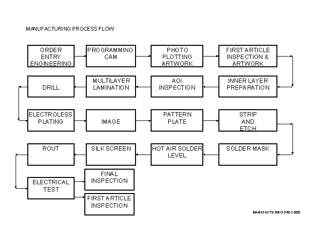
ORDER ENTRY / ENGINEERING PLANNING

 
  • Data package analyzed
  • Customer contact if required
  • Control number assigned
  • Panel layout determined
  • Multilayer stackup is selected
  • Traveler initiated
  • Material ordered
  • Inventory updated
Order Processing (13778 bytes)

Order Entry

Front End Engineering (12299 bytes)

Engineering


PROGRAMMING AND CAM

 
  • Gerber data is used to "cam" the job
  • Step and repeat the data for panelization
  • Program for drill and rout
  • Prepare cam data for photo-plotting
  • Prepare data for aoi and test
  • Manual jobs(without data) are bombsighted
CAM Operations (13244 bytes)
Programming and CAM

PHOTO-PLOTTING AND ARTWORK

F/A DRILL INSPECTION & ARTWORK INSPECTION

SHEAR AND PIN

INNER LAYER PREPARATION

 
  • Layers are cleaned and coated with dry film
  • Circuit image(negative) is printed on dry film
  • Image is developed
  • Layers are etched to remove unwanted copper
  • Dry film is removed to expose copper circuits
  • Inner layers are "aoi" inspected
  • Layers are treated with oxide to promote adhesion
Innerlayer AOI (14059 bytes)
AOI Inspection


MULTILAYER LAY-UP

 
  • Layers are oriented into the specified stack-up
  • Prepreg material is oriented between all of the layers
  • Multi-layer book is built containing several panels
Innerlayer pre-preg materials (12301 bytes)
Inner Layer Prepreg Materials


MULTILAYER LAMINATING

 
  • Press is loaded with several "books" of multi-layers
  • Vacuum is initiated in press
  • Temperature and pressure cycle is initiated
  • Prepreg liquefies and then gels to bond layers together
  • Cure cycle and then cool down
Daylight press (14004 bytes)

Daylight Press

Vacuum press (13568 bytes)

Multilayer Laminating Vacuum Press


DRILL

 
  • Multi-layers and double sided boards are drilled
  • Drill mylar(generated with the f/a) is used to check
  • Stack height is based on product and drill size
  • Drill bits are inspected and hit count is controlled
Drill Machine (13170 bytes)

Drill

ELECTROLESS

IMAGE


PATTERN PLATE

 
  • Imaged panel is electrolytic plated with copper
  • The circuit pattern and the holes are plated
  • Dry film resists plating between circuits
  • Circuit pattern and holes are plated with tin
  • Tin acts as an etch resist to protect circuits and holes
Pattern plate line (14723 bytes)

Pattern Plate Line

Close up of pattern plate line (14912 bytes)

Pattern Plate Close-Up

Plating fixture (14383 bytes)

Pattern Plate fixture and panel features


STRIP AND ETCH

 
  • Panels are processed through a film strip and etch
  • Ammoniacal etch removes all of the unwanted copper
  • Tin is removed leaving bare copper and laminate
  • If a gold or tin nickel finish is desired, the tin process is eliminated and the gold or tin nickel is the etch resist

Etching line (14166 bytes)

Strip and Etch


SOLDERMASK

 
  • The soldermask screen is made from the film
  • Panel surface is scrubbed
  • The bare copper panels are coated with soldermask ink
  • Panels are cured
  • In the case of lpi, panels are printed, developed, & cured
Soldermask screen printer (12538 bytes)
Soldermask Application


HOT AIR SOLDER LEVEL

 
  • Panels are coated with activating flux
  • Panels are inserted into the molten solder chamber
  • Solder fills the holes and covers the surface
  • Excess solder is blown out of holes and from surface
  • Thin coating of solder is left on the surface & in holes
Hot air solder leveling machine (12807 bytes)

Hot Air Solder

SILK-SCREEN


ROUTING

 
  • The individual circuit boards are removed from panel
  • Removal is done with numerically controlled router
  • Individual boards are sized per the specification
Routing machine (14123 bytes)
Routing


ELECTRICAL TEST

 
  • The individual board is tested electrically
  • Test is either reference or net-list
  • The test detects shorts and opens
Electrical test fixture (14210 bytes)

Electrical Test


FINAL INSPECTION

 
  • Each board is inspected to ensure compliance with spec
  • Samples are taken for all mechanical measurements
  • Visual attributes are 100% inspected
  • During the manufacturing process, various inspections are made to ensure that the process is intact and product is meeting the requirements.
Final inspection (13725 bytes)
Final Inspection


FIRST ARTICLE INSPECTION

 
  • PTHs are potted, cross sectioned and examined to ensure compliance with spec
  • Panels are placed on the Perfect Test equipment to check layer registration
PTH Cross section examination (13951 bytes)
First Article Inspection
Perfect Test machine (11254 bytes)

Perfect Test


More Pictures

Kindly provided courtesy of Circuit Express (11254 bytes)CIRCUIT EXPRESS, INC.