Slide 19 of 26
Notes:
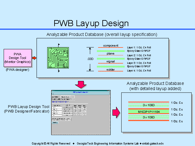
- Only preliminary information about the layup of the board was mapped from AP210 to the APM.
- However, this information is not sufficient to perform the analyses, as they require more detailed information about the layup of the board, such as the sequence of layers and their material properties and thicknesses.
- This information is not provided by the electrical engineer who designed the PWA, because he or she is not concerned with that level of detail.
- Instead, this information is supplied later in the design process by the PWB fabricator, who chooses the specific combination of layers used to build the PWB.
- For this purpose, the PWB fabricator uses the PWB Layup Design Tool (as shown in this slide).
- As shown here, once the PWB fabricator specifies the detailed layup in the PWB Layup Design Tool, the APM is augmented with the more detailed layup information.

